

Application of Neural-symbol Model Based on Stacked Denoising Auto-encoders in Wafer Map Defect Recognition
-
摘要: 深度神经网络是具有复杂结构和多个非线性处理单元的模型, 通过模块化的方式分层从数据提取代表性特征, 已经在晶圆缺陷识别领域得到了较为广泛的应用. 但是, 深度神经网络在应用过程中本身存在“黑箱”和过度依赖数据的问题, 显著地影响深度神经网络在晶圆缺陷识别的工业可应用性. 提出一种基于堆叠降噪自编码器的神经–符号模型. 首先, 根据堆叠降噪自编码器的网络特点采用了一套符号规则系统, 规则形式和组成结构使其可与深度神经网络有效融合. 其次, 根据 网络和符号规则之间的关联性提出完整的知识抽取与插入算法, 实现了深度网络和规则之间的知识转换. 在实际工业晶圆表面图像数据集WM-811K上的试验结果表明, 基于堆叠降噪自编码器的神经–符号模型不仅取得了较好的缺陷探测与识别性能, 而且可有效提取规则并通过规则有效描述深度神经网络内部计算逻辑, 综合性能优于目前经典的深度神经网络.Abstract: Deep neural network is a model with complex structure and multiple non-linear processing units. It has achieved great successes in wafer map pattern recognition through deep feature learning. In order to solve the problem of unexplained “black box” and excessive dependence on data in the applications of deep neural networks, this paper proposes a neural-symbol model based on a stacked denoising auto-encoders. Firstly, the symbolic rule system is designed according to the characteristics of stacked denoising auto-encoders. Secondly, according to the inner association between the network and the rules, a knowledge extraction and insertion algorithm is proposed to describe the deep network and improve the performance of the network. The experimental results on the industrial wafer map image set WM-811K show that the neural-symbol model based on stacked denoising auto-encoders not only achieves better defect pattern recognition performance, but also can effectively describe the internal logic of the neural network through rules, and its comprehensive performance is better than that of the current classical classification model.
-
Key words:
- Wafer map defect /
- deep learning /
- stacked denoising auto-encoders /
- symbolic rule /
- knowledge discovery
-
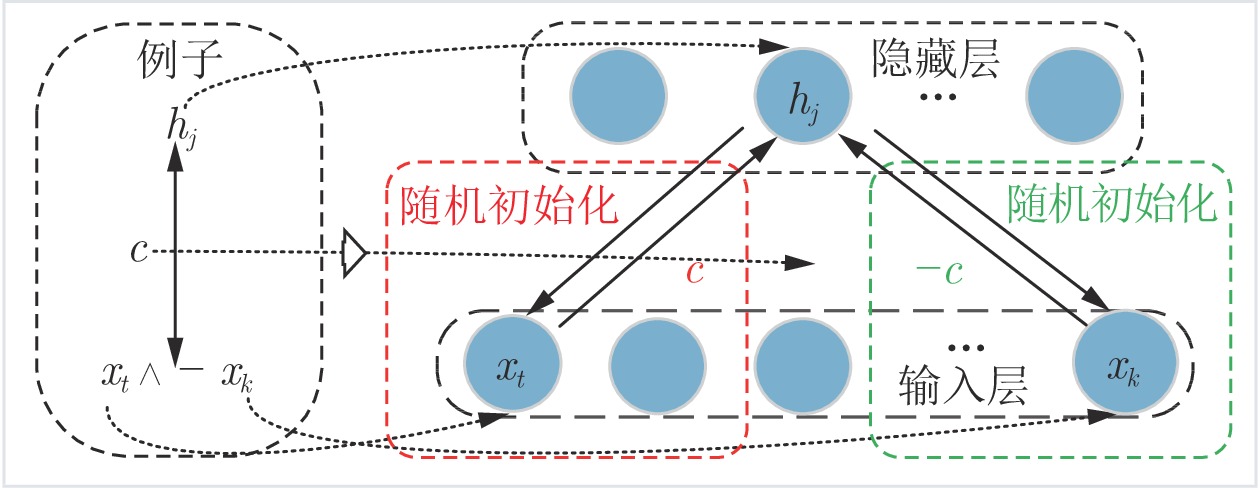
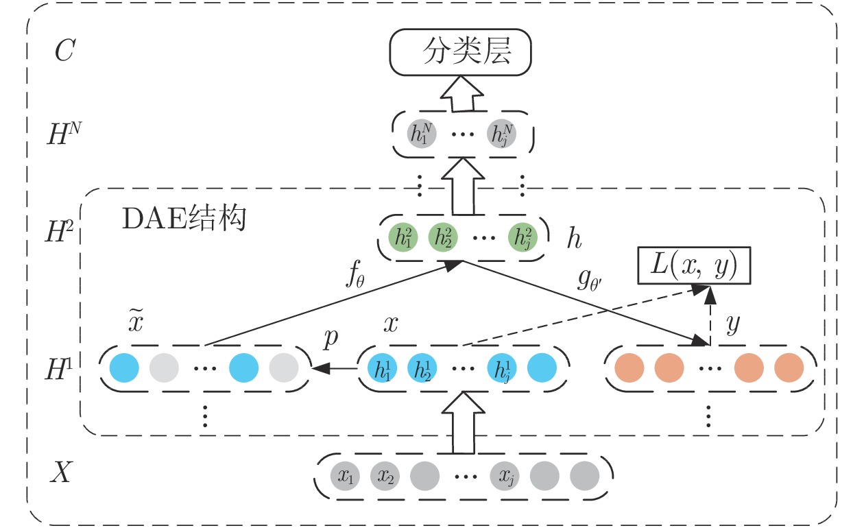
图 3 置信度规则初始化网络过程示意图
Fig. 3 The process of network initialization base on confidence rule
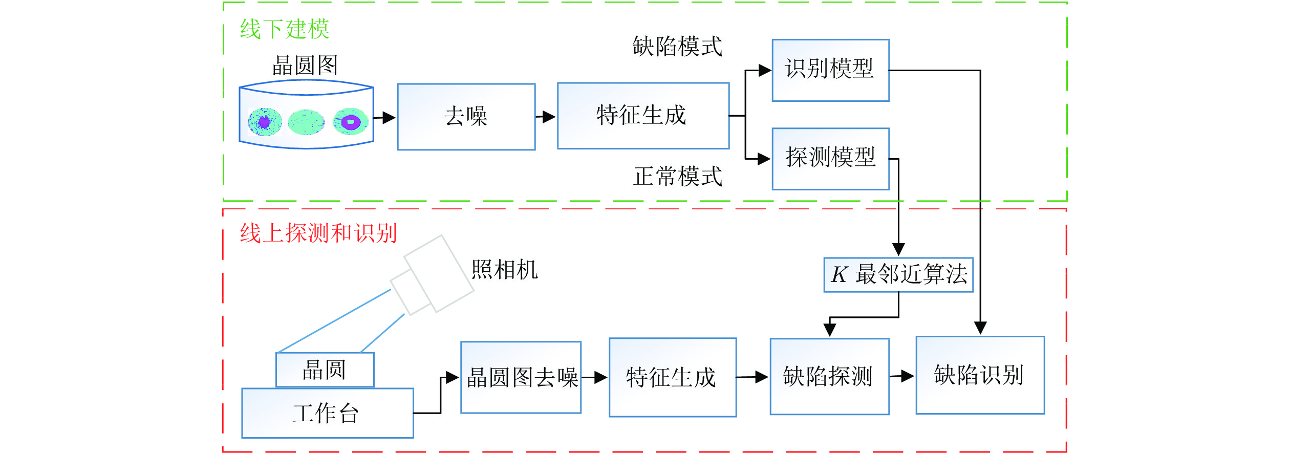
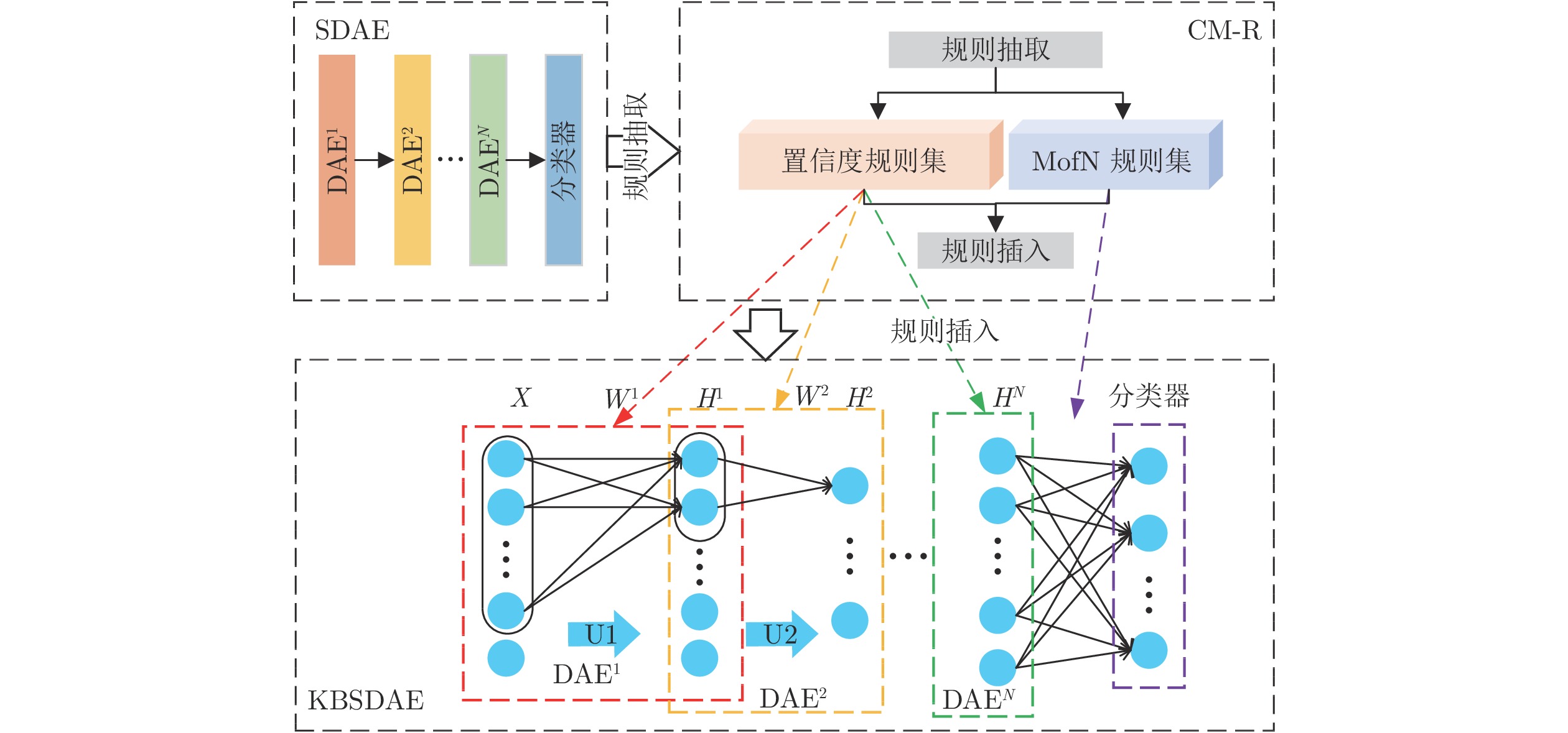
图 5 基于KBSDAE的晶圆表面缺陷识别系统
Fig. 5 Wafer surface defect recognition system based on KBSDAE
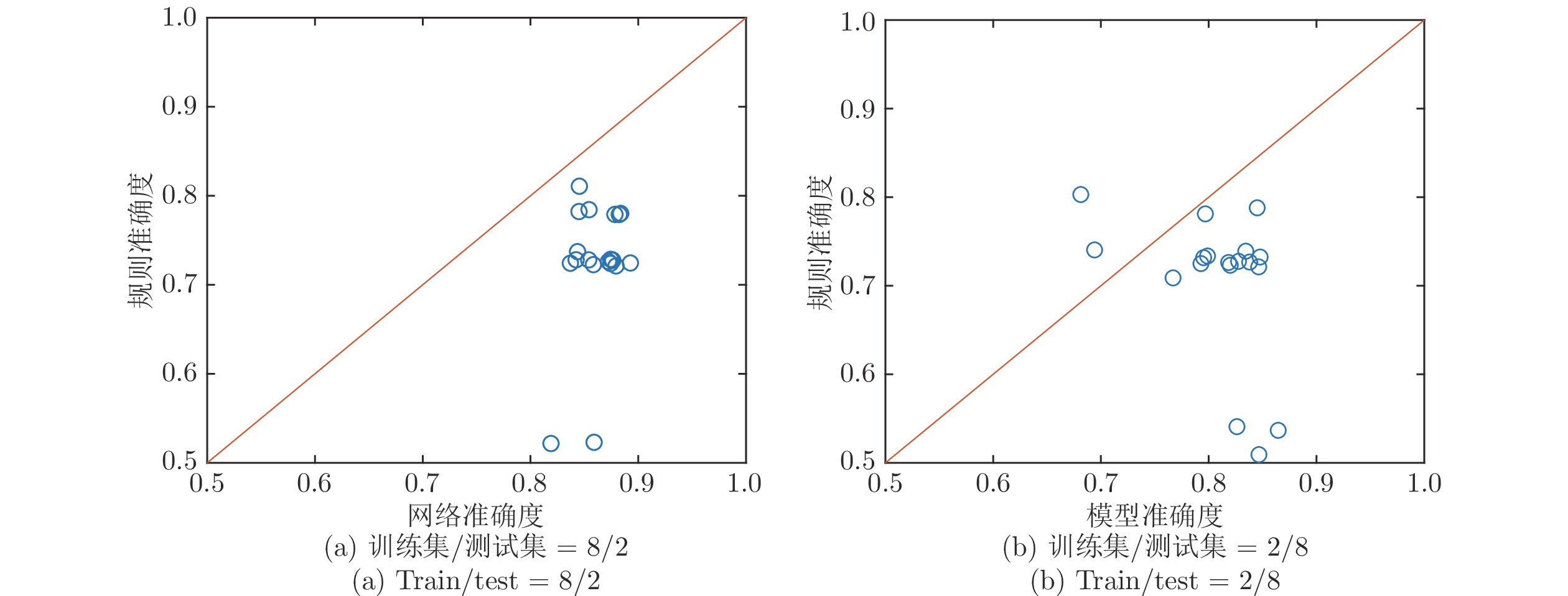
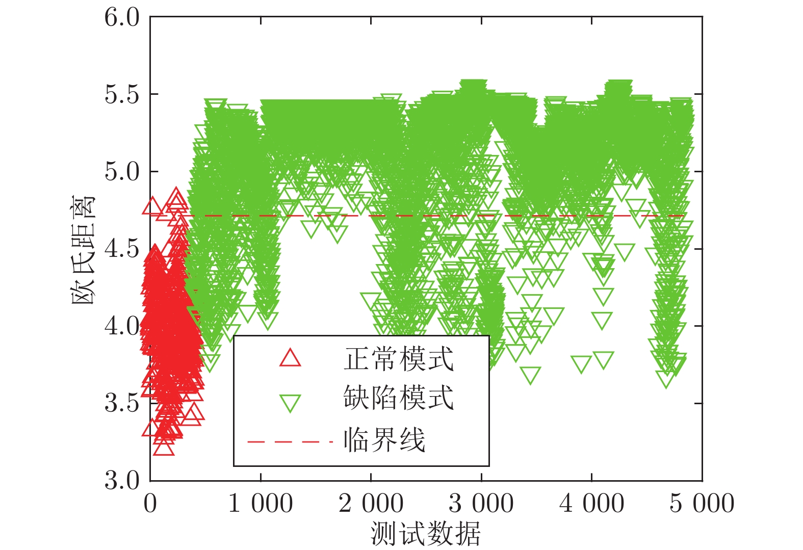
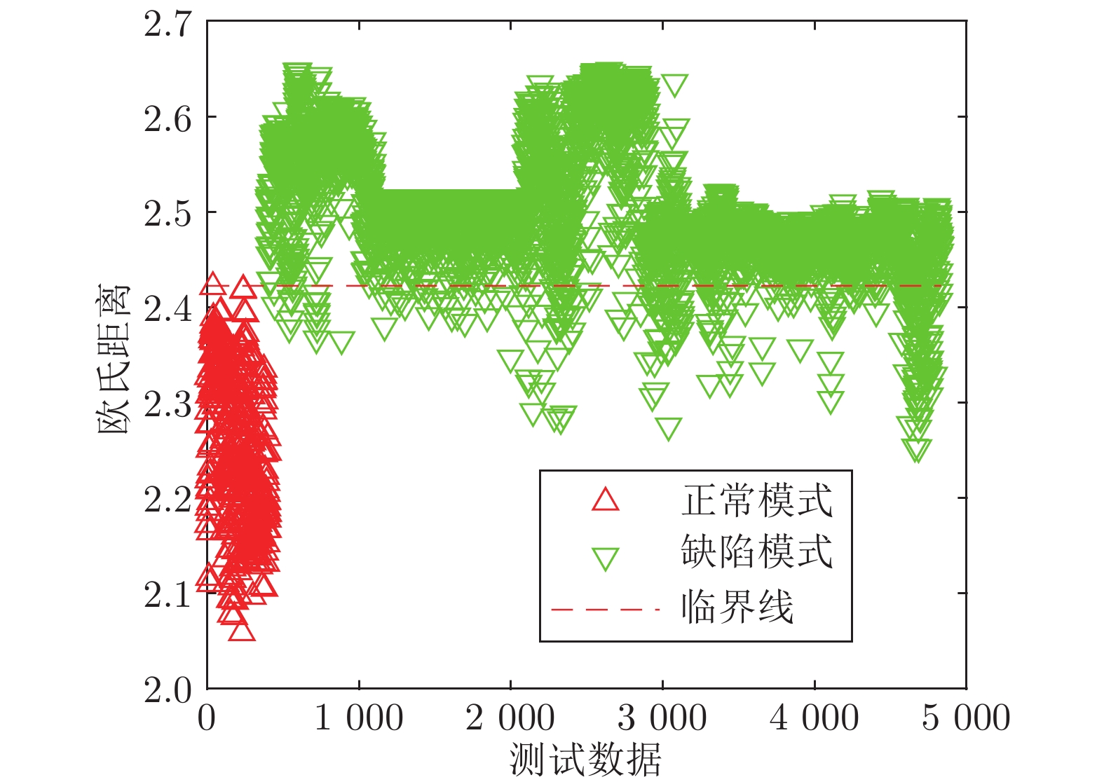
图 12 SDAE和相应的符号规则的晶圆表面缺陷识别率对比
Fig. 12 Comparison of wafer defect recognition rates between SDAE and corresponding rules
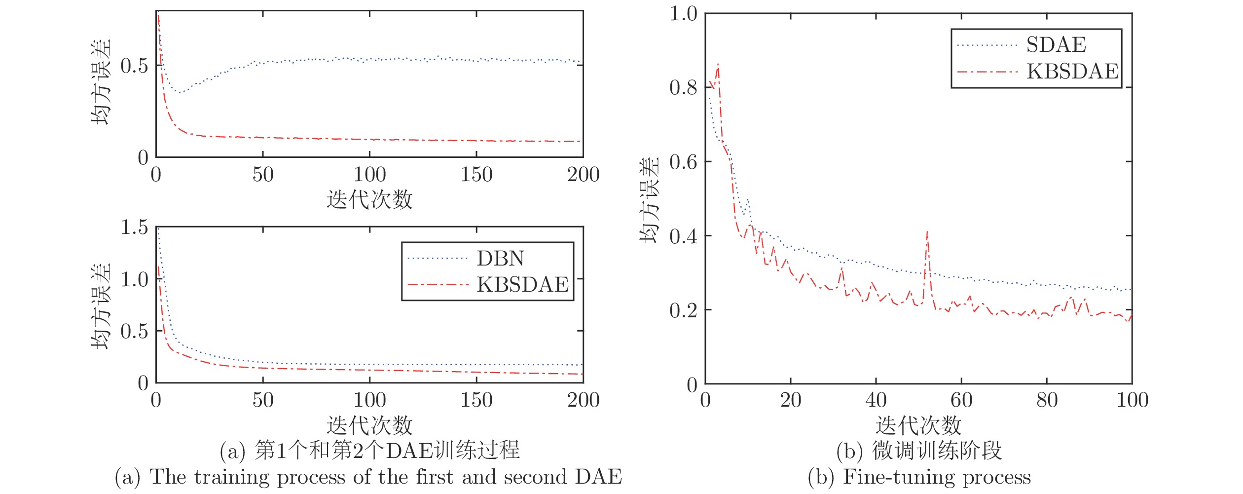
图 13 KBSDAE和SDAE训练过程的均方误差变化对比
Fig. 13 Comparison of mean square errors of KBSDAE and SDAE training processes

图 15 不同微调训练步数的SDAE与KBSDAE分类性能比较
Fig. 15 Comparison of classification performances between SDAE and KBSDAE with different fine-tuning steps
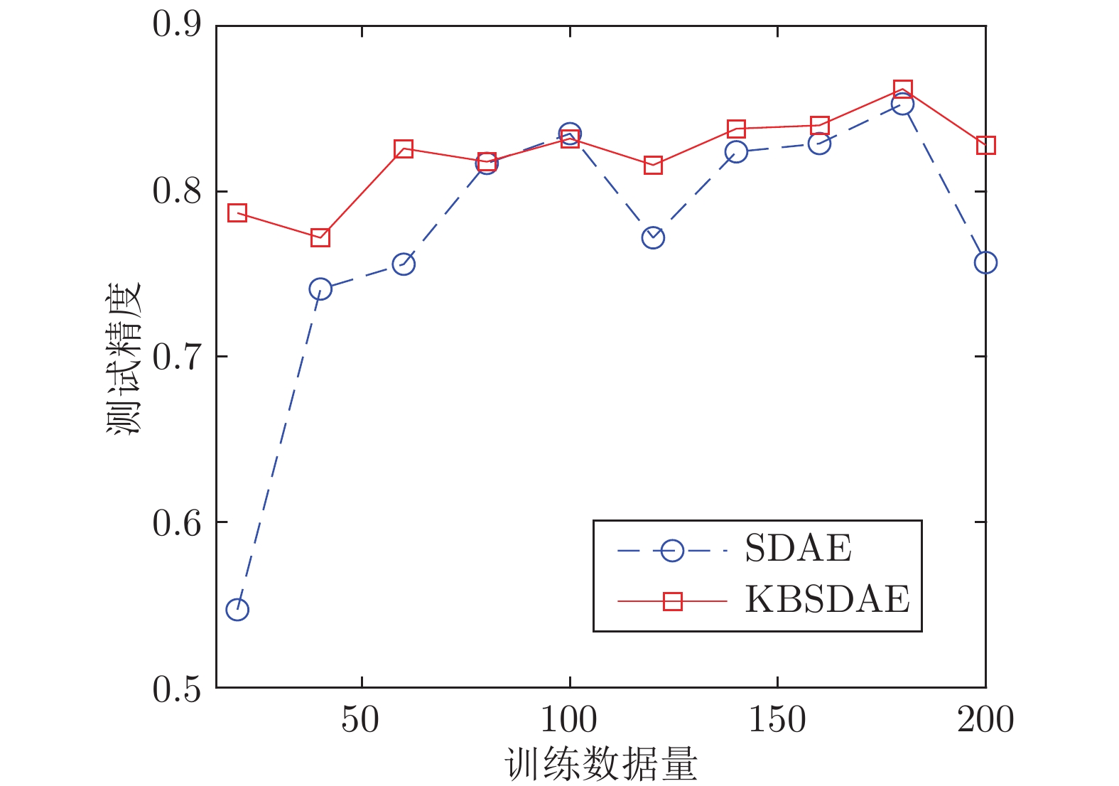
图 16 不同训练数据量下的 KBSDAE 与 SDAE 识别性能比较
Fig. 16 Comparison of classification performances between KBSDAE and SDAE with different training data volumes
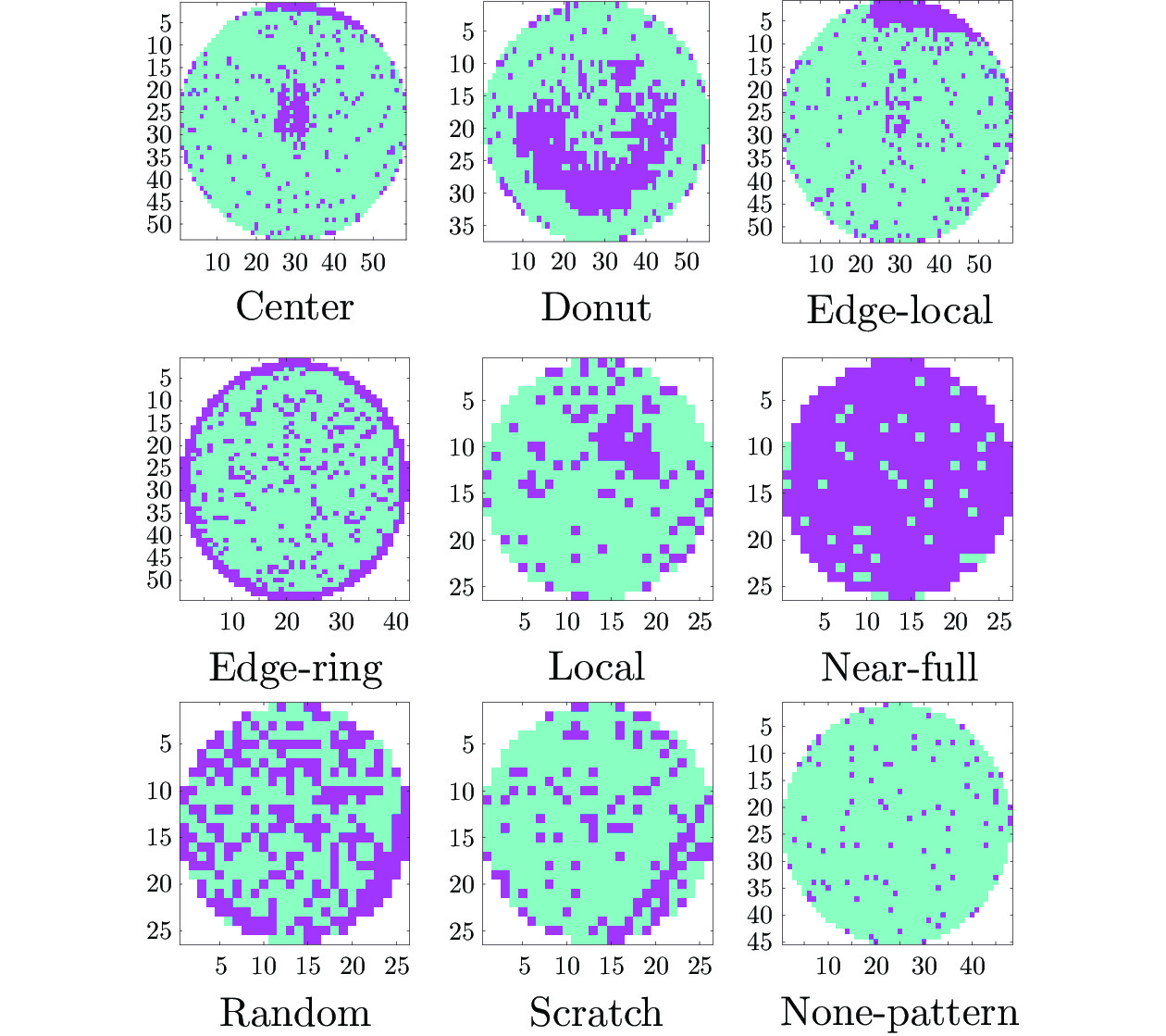
表 1 晶圆图像特征集
Table 1 Wafer map feature set
特征类别 特征集 几何特征 区域特征、线性特征、Hu 不变矩 灰度特征 平均值、方差、歪斜度、峰值、能量、熵 纹理特征 能力、对比度、相关性、均匀度、熵 投影特征 峰值、平均幅值、均方根幅值、投影波形特性、
投影峰值、投影脉冲 下载: 导出CSV
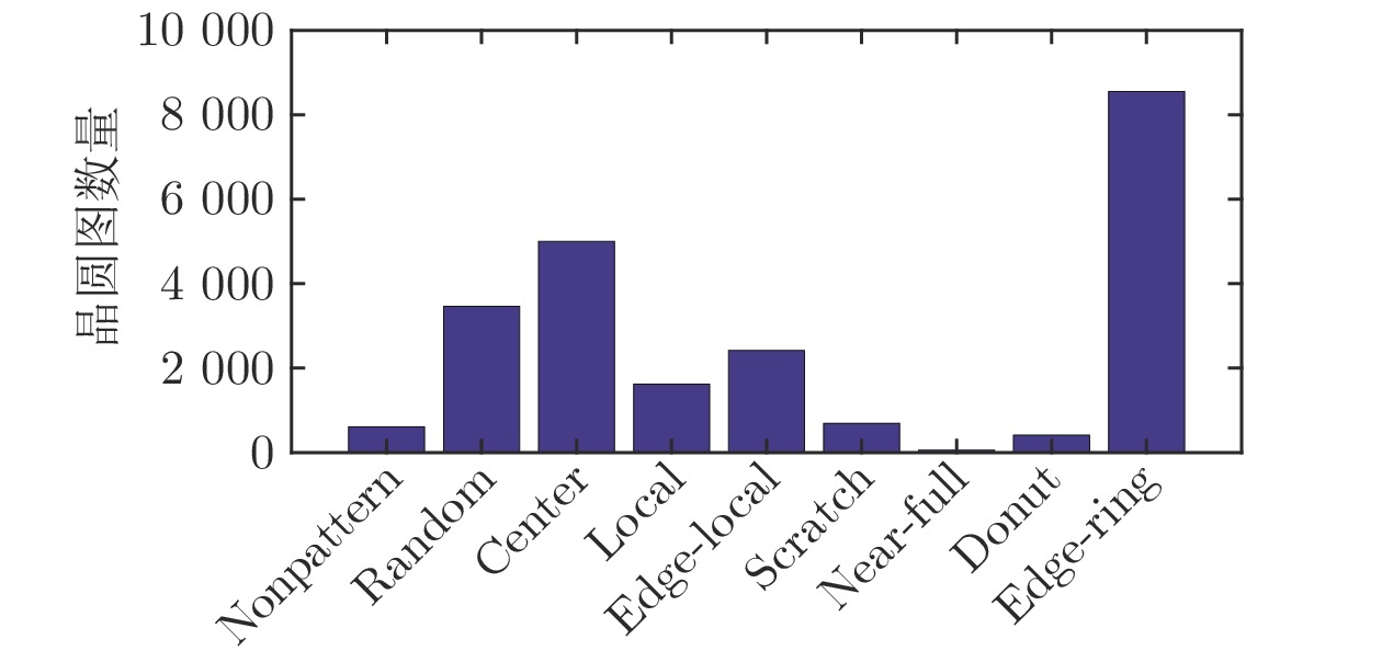
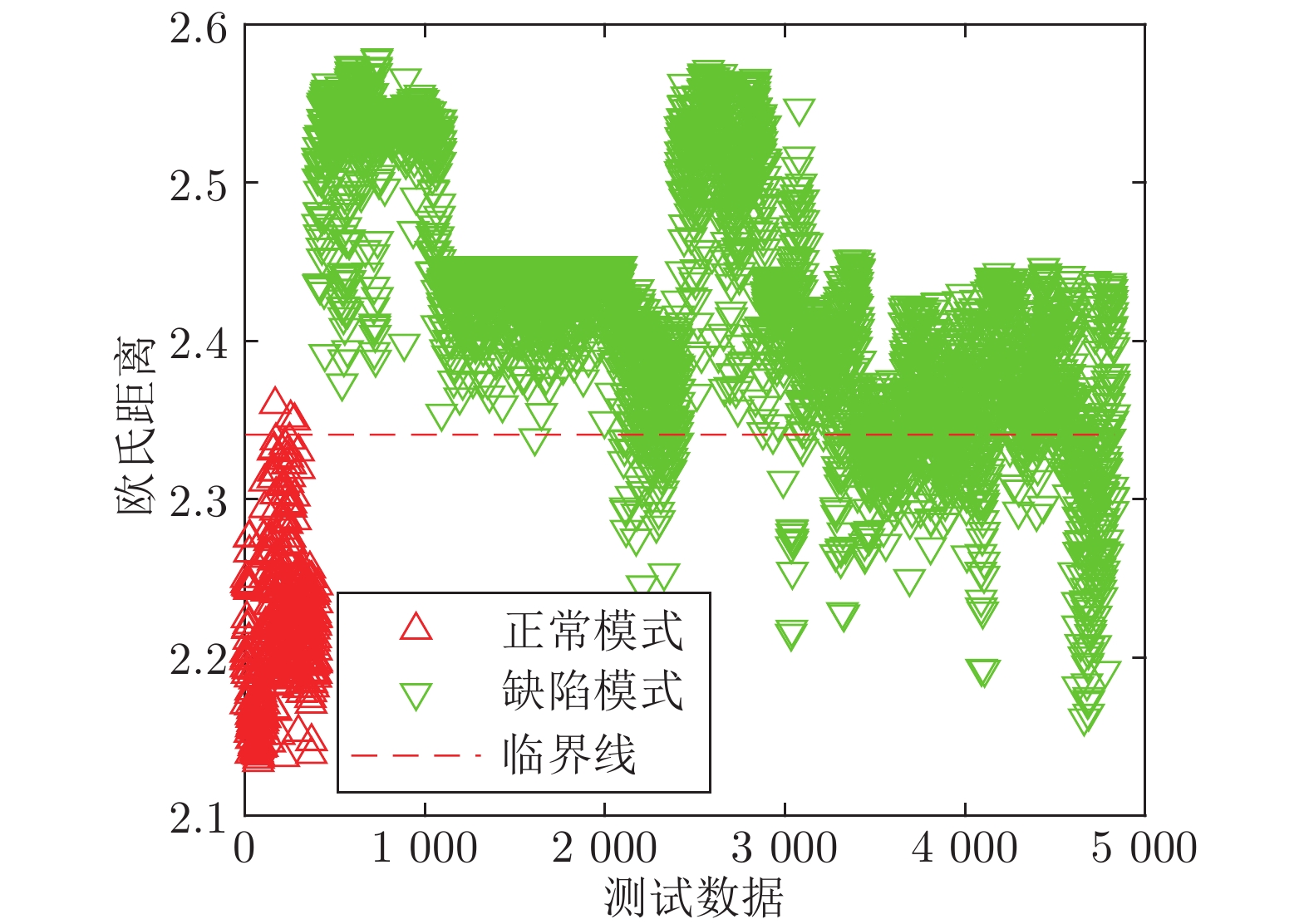
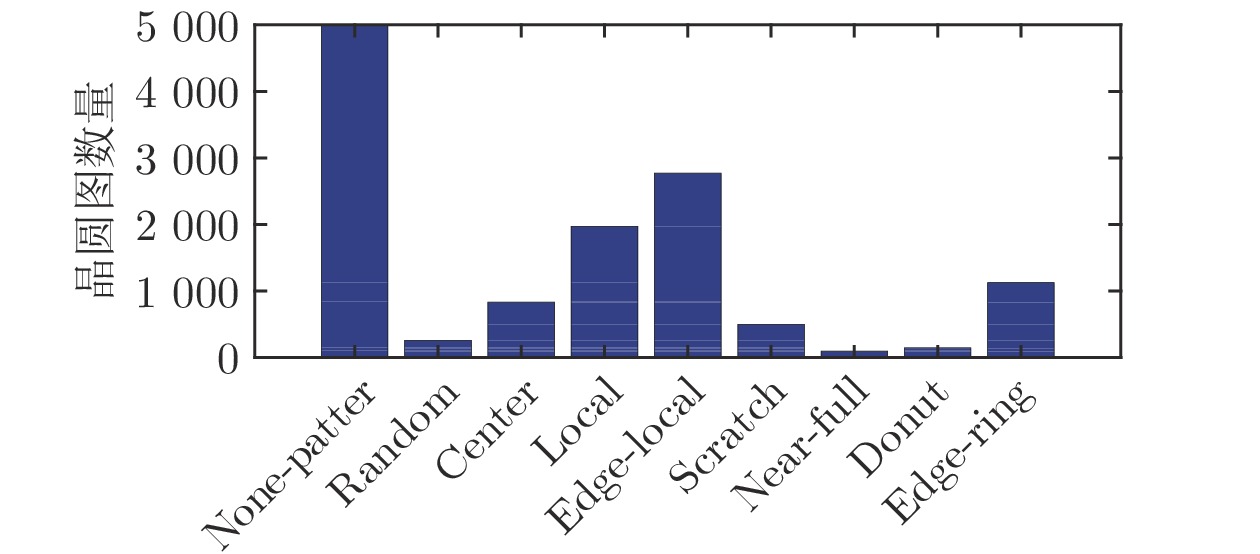
表 2 3种控制图的缺陷探测率 (%)
Table 2 Defect detection capabilities of three control charts (%)
模式 原始数据 SDAE KBSDAE Random 62.90 100 97.54 Center 99.40 99.90 97.20 Local 58.02 81.48 88.58 Edge-local 85.03 100 98.75 Scratch 99.27 98.54 86.86 Near-full 0.00 0.00 100 Donut 7.41 97.53 81.48 Edge-ring 91.10 67.19 90.86 平均值 70.89 80.58 93.52
下载: 导出CSV
表 3 部分置信度符号规则
Table 3 Part of Confidence Rule
DAE 置信度规则 DAE 1 $\begin{aligned} & {\rm{0} }{\rm{.55} }:h_{ 2}^1 \Leftrightarrow {x_{\rm{1} } } \wedge \neg {x_{\rm{2} } } \wedge \neg {x_4} \wedge {x_5} \wedge \cdots \wedge {x_{21} } \wedge \neg {x_{22} } \wedge {x_{23} } \wedge \neg {x_{25} } \wedge \cdots \wedge \neg {x_{ {\rm{49} } } } \wedge {x_{50} } \wedge \neg {x_{51} } \\ & 0.65:h_{42}^1 \Leftrightarrow \neg {x_{\rm{1} } } \wedge \neg {x_{\rm{2} } } \wedge \neg {x_3} \wedge {x_4} \wedge \neg {x_5} \wedge \cdots \wedge \neg {x_{24} } \wedge {x_{25} } \wedge \cdots \wedge \neg {x_{ {\rm{49} } } } \wedge \neg {x_{50} } \wedge {x_{51} } \\ & {\rm{0} }{\rm{.56} }:h_{79}^1 \Leftrightarrow {x_{\rm{1} } } \wedge {x_3} \wedge \neg {x_4} \wedge \cdots \wedge {x_{21} } \wedge {x_{22} } \wedge {x_{23} } \wedge \neg {x_{24} } \wedge \neg {x_{25} } \wedge \cdots \wedge {x_{ {\rm{49} } } } \wedge {x_{50} } \wedge {x_{51} } \\ \end{aligned}$ DAE 2 $0.72:h_9^2 \Leftrightarrow \neg h_{\rm{2}}^1 \wedge \neg h_5^1 \wedge h_{\rm{7}}^1 \wedge \neg h_{10}^1 \wedge \neg h_{11}^1 \wedge \neg h_{12}^1 \wedge \cdots \wedge \neg h_{41}^1 \wedge h_{42}^1 \wedge \cdots \wedge \neg h_{77}^1 \wedge \neg h_{78}^1 \wedge \neg h_{{\rm{79}}}^1$
下载: 导出CSV
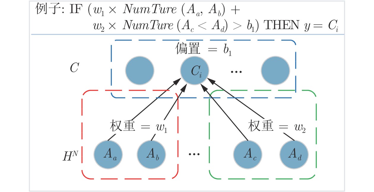
表 4 部分MofN规则
Table 4 Part of MofN Rule
分类 MofN 规则 类别 1$(C1)$ ${\rm{IF} }\;0.68\times{ {NumberTure}\; }({ {h} }_2^2,{ {h} }_3^2,{ {h} }_4^2,{ {h} }_5^2,{ {h} }_6^2,{ {h} }_7^2,{ {h} }_9^2,{ {h} }_{10}^2,{ {h} }_{12}^2,{ {h} }_{13}^2) - 1.35\times{ { {NumberTure} }\; }({ {h} }_1^2,{ {h} }_8^2,{ {h} }_{11}^2,{ {h} }_{14}^2,{ {h} }_{15}^2) > 0.75\;{ {{\rm{THEN}}} }\;{ {C} }1$ 类别 4$(C4)$ ${\rm{IF} }\;3.45\times{{NumberTure} \;}({ {h} }_5^2,{ {h} }_6^2,{ {h} }_7^2,{ {h} }_8^2) - 0.87\times{{NumberTure} \;}({ {h} }_1^2,{ {h} }_2^2,{ {h} }_3^2,{ {h} }_4^2,{ {h} }_9^2,{ {h} }_{10}^2,{ {h} }_{11}^2,{ {h} }_{12}^2,{ {h} }_{13}^2,{ {h} }_{14}^2,{ {h} }_{15}^2) > 4.73\;{\rm{THEN} }\;{ {C} }4$ 类别 5$(C5)$ ${\rm{IF} }\;0.85\times{ {NumberTure}\; }({ {h} }_2^2,{ {h} }_4^2,{ {h} }_5^2,{ {h} }_6^2,{ {h} }_7^2,{ {h} }_8^2,{ {h} }_9^2,{ {h} }_{10}^2,{ {h} }_{12}^2,{ {h} }_{15}^2) - 1.76\times{ { { {NumberTure} } }\; }({ {h} }_1^2,{ {h} }_3^2,{ {h} }_{11}^2,{ {h} }_{13}^2,{ {h} }_{14}^2,) > 1.44\;{\rm{THEN} }\;{{C} }5$
下载: 导出CSV
表 5 基于 KBSDAE 的晶圆缺陷识别率
Table 5 Recognition rates of defects in wafers based on KBSDAE
模式 Random Center Local Edge-local Scratch Near-full Donut Edge-ring Random 0.91 0 0.06 0 0 0 0 0.03 Center 0.01 0.99 0 0 0 0 0 0 Local 0.01 0.01 0.81 0 0.09 0 0 0.08 Edge-local 0 0.02 0 0.98 0 0 0 0 Scratch 0 0 0.03 0.02 0.83 0 0 0.12 Near-full 0 0 0.01 0 0.25 0.84 0 0 Donut 0 0 0 0.13 0 0 0.87 0 Edge-ring 0 0 0 0 0.02 0 0 0.98
下载: 导出CSV
表 6 结构规则超参数敏感性分析
Table 6 Model hyperparameter sensitivity analysis
隐藏层数 隐节点数 置信度规则数 分类规则数 准确度 (%) 1 20 + 5 1/2 1 89.37 1/2 88.70 1/4 87.57 1/3 1 89.00 1/2 88.80 1/4 88.57 1/5 1 89.80 1/2 88.97 1/4 87.67 2 80, 15 + 5 1/2 1 86.27 1/2 90.02 1/4 89.00 1/3 1 90.00 1/2 91.56 1/4 89.78 1/5 1 90.00 1/2 88.13 1/4 88.90 3 80, 30, 15 + 5 1/2 1 84.23 1/2 89.37 1/4 89.20 1/3 1 83.47 1/2 87.33 1/4 88.07 1/5 1 84.23 1/2 88.62 1/4 89.05
下载: 导出CSV
表 7 各种学习模型的晶圆缺陷识别率 (%)
Table 7 Wafer defect recognition rates for various learning models (%)
数据集 WM-811K 仿真 DBN 80.84 86.34 SDAE 89.87 91.28 SSAE 86.6 87.96 BPNN 80.71 89.25 DenseNet 88.6 90.69 ResNet 86.53 91.89 GoogleNet 74.32 90.63 SVMG 72.54 78.86 SYM-DBN 85.63 90.58 INSS-KBANN 81.96 92.78 JLNDA 90.4 90.84 KBSDAE 91.14 95.28
下载: 导出CSV
-
[1] Hansen M H, Nair V N, Friedman D J. Monitoring wafer map data from integrated circuit fabrication processes for spatially clustered defects. Technometrics, 1997, 39(3): 241-253. [2] Hsieh K L, Tong L I, Wang M C. The application of control chart for defects and defect clustering in IC manufacturing based on fuzzy theory. Expert Systems with Applications, 2007, 32(3): 765-776. doi: 10.1016/j.eswa.2006.01.050 [3] Hess C, Weiland L H. Extraction of wafer-level defect density distributions to improve yield prediction. IEEE Transactions on Semiconductor Manufacturing, 1999, 2(2): 175−183 [4] Friedman D J, Hansen M H, Nair V N, et al. Model-free estimation of defect clustering in integrated circuit fabrication. IEEE Transactions on Semiconductor Manufacturing, 1997, 10(3): 344-359. doi: 10.1109/66.618208 [5] Yuan T, Kuo W. Spatial defect pattern recognition on semiconductor wafers using model-based clustering and Bayesian inference. European Journal of Operational Research, 2008, 190(1): 228−240 [6] 余建波, 卢笑蕾, 宗卫周. 基于局部与非局部线性判别分析和高斯混合模型动态集成的晶圆表面缺陷探测与识别[J]. 自动化学报, 2016, 42(01): 47-59.Yu jian-bo, Lu xiao-lei, Zong zhou-wei. Wafer Defect Detection and Recognition Based on Local and Nonlocal Linear Discriminant Analysis and Dynamic Ensemble of Gaussian Mixture Models. Acta Automatic sinica, 2016, 42(01): 47-59. [7] Huang C J. Clustered defect detection of high quality chips using self-supervised multilayer perceptron. Expert Systems with Applications, 2007, 33(4), 996-1003. doi: 10.1016/j.eswa.2006.07.011 [8] Baly R, Hajj H. Wafer classification using support vector machines, IEEE Transactions on Semiconductor Manufacturing, 2012, 25(3): 373−383 [9] Xie L, Huang R, Gu N, Zhi C. A novel defect detection and identification method in optical inspection. Neural Computing and Applications, 2014, 24(7-8): 1953-1962. doi: 10.1007/s00521-013-1442-7 [10] Chao L C, Tong L I. Wafer defect pattern recognition by multi-class support vector machines by using a novel defect cluster index. Expert Systems with Applications, 2009, 36(6): 10158-10167. doi: 10.1016/j.eswa.2009.01.003 [11] Nakazawa T, & Kulkarni D V. Wafer map defect pattern classification and image retrieval using convolutional neural network. IEEE Transactions on Semiconductor Manufacturing, 2018, 31(2): 309-314. [12] 邡鑫, 史峥. 基于卷积神经网络的晶圆缺陷检测与分类算法[J]. 计算机工程, 2018, 44(08): 218-223.Fang Xin, Shi Zheng. Wafer defect detection and classification algorithms based on convolutional neural network. Computer Engineering, 2018, 44(8): 218-223. [13] Yu J B. Enhanced stacked denoising utoencoder-based feature learning for recognition of wafer map defects. in IEEE Transactions on Semiconductor Manufacturing, 2019, 32 (4): 613-624. doi: 10.1109/TSM.2019.2940334 [14] Lee H, Kim Y, Kim C O. A deep learning model for robust wafer fault monitoring with sensor measurement noise. in IEEE Transactions on Semiconductor Manufacturing, 2017, 30(1): 23-31. doi: 10.1109/TSM.2016.2628865 [15] 孙晨, 周志华, 陈兆乾. 神经网络规则抽取研究[J]. 计算机应用研究, 2000, 17(2): 34-37. doi: 10.3969/j.issn.1001-3695.2000.02.013Sun Chen, Zhou Zhi-hua, Chen Zhao-qian. Study on rule extraction of neural network. Application Research of Computers, 2000, 17(2): 34-37. doi: 10.3969/j.issn.1001-3695.2000.02.013 [16] Gallant S I. Connectionist expert systems. Communications of the ACM, 1988, 31(2): 152-169. doi: 10.1145/42372.42377 [17] Towell G G, Shavlik J W. Knowledge-based artificial neural networks. Artificial Intelligence, 1994, 70(1-2): 119-165. doi: 10.1016/0004-3702(94)90105-8 [18] Garcez A S A, Zaverucha G. The Connectionist Inductive Learning and Logic Programming System. Applied Intelligence, 1999, 11(1): 59-77. doi: 10.1023/A:1008328630915 [19] Garcez A A, Gori M, Lamb L C, Serafini L. Neural-symbolic computing: An effective methodology for principled integration of machine learning and reasoning. arXiv preprint, 2019, arXiv: 1905.06088 [20] Odense S, Garcez A A. Extracting m of n rules from restricted boltzmann machines. In: Proceedings of the 2017 International Conference on Artificial Neural Networks. Alghero, Italy: Springer, 2017. 120−127 [21] Tran S N, Garcez A S D. Deep Logic Networks: Inserting and Extracting Knowledge from Deep Belief Networks. IEEE Transactions on Neural Networks & Learning Systems, 2018, 29(2): 246-258. [22] 刘国梁, 余建波. 知识堆叠降噪自编码器. 自动化学报, 2022, 48(3): 774−786Liu Guo-Liang, Yu Jian-Bo. Knowledge based stacked denoising autoencoder. Acta automatic sinica, 2022, 48(3): 774−786 [23] Hitzler P, Bianchi F, Ebrahimi M, & Sarker M K. Neural-symbolic integration and the semantic web. Sprachwissenschaft, 2020, 11(1), 3–11. [24] Bennetot A, Laurent J L, Chatila R, Díaz-Rodríguez N. Towards explainable neural-symbolic visual reasoning. ArXiv Prepr-int, 2019, ArXiv: 1909.09065 [25] Li S, Xu H, Lu Z. Generalize symbolic knowledge with neural rule engine. arXiv preprint, 2018, arXiv: 1808.10326v1 [26] Sukhbaatar S, Szlam A, Weston J, & Fergus R. End-To-End memory networks. ArXiv Preprint, 2015, ArXiv: 1503.08895 [27] Sawant U, Garg S, Chakrabarti S, Ramakrishnan G. Neural architecture for question answering using a knowledge graph and web corpus. Information Retrieval Journal, 2019, 22(3−4): 324− 349 [28] Liang C, Berant J, Le Q, Forbus K D, Ni L. Neural symbolic machines: Learning semantic parsers on freebase with weak supervision. arXiv preprint, 2016, arXiv: 1611.00020 [29] Salha G, Hennequin R, & Vazirgiannis M. Keep it simple: Graph autoencoders without graph convolutional networks. arXiv preprint, 2019, arXiv: 1910.00942 [30] Salha G, Hennequin R, Tran V A, & Vazirgiannis M. A degeneracy framework for scalable graph autoencoders. arXiv prepr-int, 2019, arXiv: 1902.08813 [31] Vincent P, Larochelle H, Bengio Y, Manzagol P A. Extracting and composing robust features with denoising autoen-coders. In: Proceedings of the 25th International Conferenceon Machine Learning. Helsinki, Finland: 2008. 1096−1103 [32] Towell G G, Shavlik J W. Extracting refined rules from knowledge-based neural networks. Machine learning, 1993, 13(1): 71-101. [33] Szegedy C, Liu W, Jia Y, Sermanet P, Rabinovich A. Going deeper with convolutions. In: Proceedings of the 2015 IEEE Conference on Computer Vision and Pattern Recognition. Wash-ington DC, USA: 2015. 1–9 [34] Tran S N, Garcez A S D. Knowledge extraction from deep Belief networks for images. In: Proceedings of the 2013 IJCAI-Workshop Neural-Symbolic Learn. Washington DC, USA: 2013. 1–6 [35] Wang C H, Kuo W, Bensmail H. Detection and classification of defect patterns on semiconductor wafers. IIE Trans-actions, 2006, 38(12): 1059-1068. doi: 10.1080/07408170600733236 [36] Wu M J, Jang J S R, and Chen J L. Wafer map failure pattern recognition and similarity ranking for large-scale data sets. IEEE Transactions on Semiconductor Manufacturing, 2015, 28(1): 1-12. doi: 10.1109/TSM.2014.2364237 [37] Valiant L G. Three problems in computer science. Journal of the ACM, 2003, 50(1): 96–99. [38] Fernando S O, Amy B. INSS: A hybrid system for constructive machine learning. Neural Computing, 1999, 28(1-3): 191-205. [39] Huang G, Liu Z, Maaten L V D, Weinberger K Q. Densely connected convolutional networks. In: Proceedings of the 2019 IEEE Conference on Computer Vision and Pattern Recognition. Honolulu, Hawaii, USA: 2017. 2261–2269 [40] He K M, Zhang X Y, Ren S Q, Sun J. Deep residual learning for image recognition. In: Proceedings of the 2016 IEEE Conference on Computer Vision and Pattern Recognition. Las Vegas, USA: 2016. 770−778 [41] Yu J, Lu X. Wafer Map defect detection and recognition using joint local and nonlocal linear discriminant analysis. IEEE Transactions on Semiconductor Manufacturing, 2016, 29(1): 33-43. doi: 10.1109/TSM.2015.2497264 [42] Di Palma F, De Nicolao G, Miraglia G, et al. Unsupervised spatial pattern classification of electrical-wafer-sorting maps in semiconductor manufacturing. Pattern recognition letters, 2005, 26(12): 1857-1865. doi: 10.1016/j.patrec.2005.03.007 -

 下载:
下载:

计量
- 文章访问数: 2194
- HTML全文浏览量: 584
- PDF下载量: 272
- 被引次数: 0
